Your everyday PCB assembly is more than just a silent contributor to modern electronic devices. It plays a pivotal role, serving as the backbone for these gadgets, providing critical mechanical support, and establishing the necessary electrical connections.
In this blog post, we'll aim to demystify PCB assembly, including taking a closer look at the differences between PCBs and PCBAs:
A PCB, short for Printed Circuit Board, refers to the actual physical printed circuit boards, which provide the mechanical support and electrical connectivity that underpins the technological world.
Typically, PCBs look like green chips adorned with copper lines and components. These boards are often made of fiberglass, copper traces, and various metallic elements, which are then assembled with epoxy and enclosed in a solder mask, giving them their distinctive appearance.
The copper paths, also known as "traces," act as the neural pathways of the PCB. They connect components from one end to another, allowing the smooth flow of electrical signals, transforming the PCB – often no larger than a thumbnail – into a highly specialized, finely-tuned piece of technology.
PCBs come in various types, each designed to meet specific requirements and applications. Understanding the different types of PCBs is crucial when determining the right fit for your project. Here are some of the most common types of PCBs:
Single-sided PCBs have a single layer of substrate and conductive material on one side. Simple and cost-effective, these are often used in applications where complexity is not a concern.
Double-sided PCBs feature conductive material on both sides of the substrate. Widely used in consumer electronics, they offer increased flexibility and allow for more space-saving and complex circuit designs.
Multi-layer PCBs, as the name suggests, consist of three or more layers of substrate separated by insulating materials. These PCBs greatly improve space efficiency, making them suitable for compact, high-performance devices and advanced machinery, such as medical equipment and servers.
Also known as Flex Circuits, Flex PCBs are designed to bend and conform to various shapes and contours. They use flexible substrate materials, like polyimide, which withstand repeated bending without losing functionality. FPCBs excel in applications with space constraints or intricate form factor requirements, including foldable cell phones, and FPCBs integrated into hinges to facilitate the flexibility and movement of laptop displays.
Rigid-Flex PCBs are a hybrid of rigid and flexible board technology. They often comprise multiple layers of flexible circuit substrates connected to one or more rigid boards. Designed to be bent during production or installation, Rigid-Flex PCBs offer design versatility, making them suitable for applications where flexibility and reliability are essential.
Metal-Based PCBs, or Metal Core PCBs (MCPCBs), have their base made from metals such as copper, aluminum, and steel alloys, which all provide unique properties for various applications. Generally speaking, these PCBs are effective solutions for thermal problems in high-density circuits.
To help you determine the right PCB, Kingstec can work with prototypes of your product design and conduct pilot runs. We are fully scalable to deliver high-volume production, and can produce multi-layer PCBs and assemblies, from 2 to 16 layers.
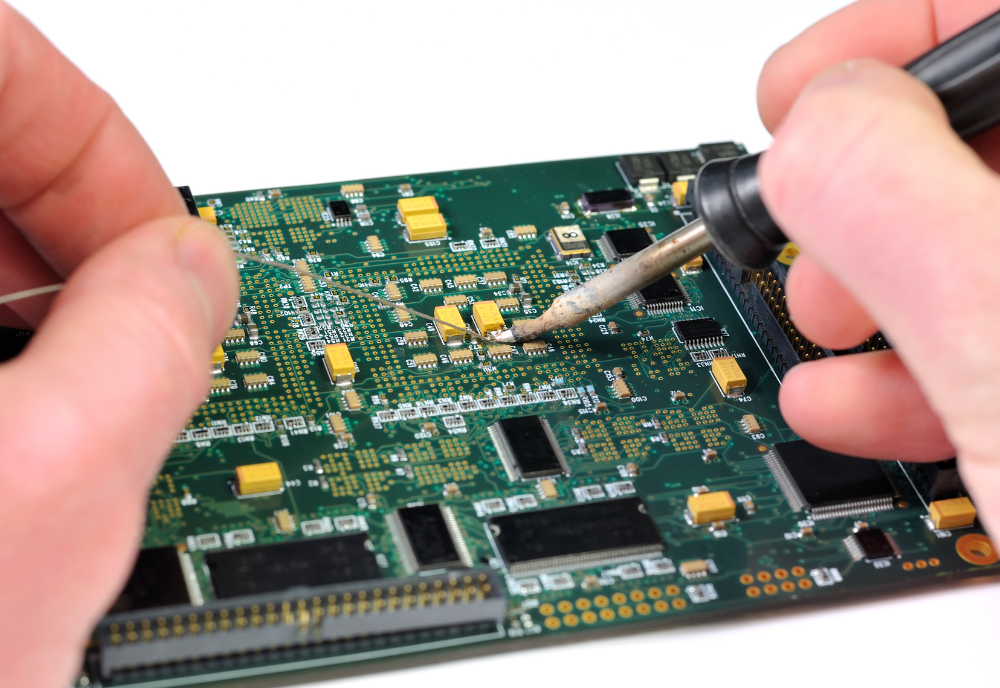
A PCBA, short for Printed Circuit Board Assembly (or Assemblies), is the complete board with electronic components (e.g. resistors, capacitors, integrated circuits, sensors, CPUs, and connectors) soldered or mounted onto the PCB. The assembly process transforms a bare PCB into a functional electronic device.
Our partner production facilities in Asia meet the highest quality standards, conforming to ISO 9001 certification.
A PCBA comprises several essential components, each with a critical role in the device's operation:
PCBAs can be categorized into different types based on the assembly technologies employed:
The PCB assembly process involves a sequence of steps to create functional electronic devices. Here's a short overview of this process:
Before assembly, a Design for Manufacturability (DFM) check is conducted to detect potential issues and identify value engineering opportunities. Kingstec’s North American engineering team can help your company clarify how design options affect production processes as needed, acting as an extension of your engineering and production departments. With our DFM process, we can help ensure your PCB is made with industry best practices.
Solder paste is applied to the designated areas on the PCB using a stencil or solder paste screen. The solder paste forms the solder joints that connect electronic components to the PCB.
Electronic components are picked up by a machine known as a pick-and-place machine and accurately placed on the solder paste-covered areas of the PCB.
The PCB undergoes reflow soldering, which involves heating it to melt the solder paste. As it cools, the solder solidifies, creating secure electrical and mechanical connections between the components and the PCB.
A solder mask insulates the PCB, while copper traces serve as electronic highways for signals and power.
Meticulous placement of electronic components is critical for PCB functionality.
The PCBA undergoes a series of rigorous testing and inspection procedures to verify its quality and functionality. These methods include manual checks for meticulous attention to detail, automated optical inspection (AOI) for high-volume production, X-ray inspection for complex PCBs, and the use of a flying lead tester to ensure proper electrical connectivity and functionality. This comprehensive testing phase guarantees that the PCBA meets the required specifications and is ready for its intended application.
Some PCBs feature Plated Through-Hole (PTH) components, which require specialized soldering methods.
The process ends with a final inspection and functional testing to ensure electrical characteristics meet specifications.
For over 40 years, Kingstec helped companies in North America and Europe grow with unmatched engineering expertise, manufacturing relationships, and global logistics experience.
We are dedicated to empowering manufacturers of all sizes, providing:
Call us today to explore how Kingstec can collaborate with your business, enabling you to develop the very highest quality PCB and PCBAs.